(China (Mainland))

Product Summary
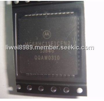
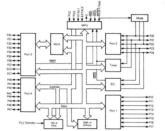
The MC68HC11E1CFN2 is a peripheral interface (SPI). It is an independent communication subsystem, allows the MCU to communicate synchronously with peripheral devices. The SPI is also capable of inter-processor communication in a multiple master system. The MC68HC11E1CFN2 system can be configured as either a master or a slave device. When configured as a master, data transfer rates can be as high as one-half the E-clock rate (1.5 Mbits per second for a 3-MHz bus frequency). When configured as a slave, data transfers can be as fast as the E-clock rate (3 Mbits per second for a 3-MHz bus frequency).
Parametrics
MC68HC11E1CFN2 absolute maximum ratings: (1)Supply voltage VDD: -0.3 to +7.0 V; (2)Input voltage VIn: -0.3 to +7.0 V; (3)Current drain per pin, ID: 25 mA; (4)Storage temperature TSTG: -55 to +150 ℃.
Features
MC68HC11E1CFN2 features: (1)M68HC11 CPU; (2)Power-saving stop and wait modes; (3)Low-voltage devices available (3.0.5 Vdc); (4)0, 256, 512, or 768 bytes of on-chip RAM, data retained during standby; (5)0, 12, or 20 Kbytes of on-chip ROM or EPROM; (6)0, 512, or 2048 bytes of on-chip EEPROM with block protect for security; (7)2048 bytes of EEPROM with selectable base address in the MC68HC811E2; (8)Asynchronous non-return-to-zero (NRZ) serial communications interface (SCI); (9)Additional baud rates available on MC68HC(7)11E20; (10)Synchronous serial peripheral interface (SPI); (11)8-channel, 8-bit analog-to-digital (A/D) converter; (12)16-bit timer system:; (13)Three input capture (IC) channels; (14)Four output compare (OC) channels; (15)One additional channel, selectable as fourth IC or fifth OC; (16)8-bit pulse accumulator; (17)Real-time interrupt circuit.
Diagrams
| Image | Part No | Mfg | Description |  |
Pricing (USD) |
Quantity | ||||
|---|---|---|---|---|---|---|---|---|---|---|
 |
 MC68HC11E1CFN2 |
|
IC MCU 512 EEPROM 2MHZ 52-PLCC |
Data Sheet |
Negotiable |
|
||||
|
MC68HC11E1CFN2R2 |
|
IC MCU 512 EEPROM 2MHZ 52-PLCC |
Data Sheet |
Negotiable |
|
||||